
News
Position:Home > News > Application

Dilong China - Find a reliable car power supply manufacturer, order DC/DC converters and onboard chargers, and then go to Dilong New Energy. Dilong has been focusing on the power supply industry for 20 years, from China to the world, professional / reliable / cost-effective, it is worth choosing!
Dilong New Energy focuses on the research and development, production and sales of on-board chargers (OBC), DCDC converters and on-board integrated machines. It is a world-renowned on-board power supplier.
The company applies the LLC resonant circuit to the vehicle charger, so that the product has the core advantages of high efficiency and high power density. We specially invited the engineers of Dilong New Energy to answer some key questions of LLC.
1. Why does LLC work in the perceptual area?
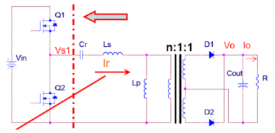
For the LLC network, there are three states of inductive, capacitive and purely resistive, which vary according to the input and load changes, as shown in the LLC equivalent model as Schematic below.
Working in the purely resistive area is the most ideal working state, because the resistive network has the highest quality factor and the best network characteristics.
Working in the capacitive region, the current leads the voltage, and the front-stage switch is easy to achieve ZCS turn-off. This region is more suitable for IGBTs.
Working in the inductive region, the voltage leads the current, and the front-stage switch is easy to realize ZVS turn-on. This region is more suitable for MOSFET.
Because MOSFETs are commonly used in small and medium power power supplies, conventional LLC topology switching power supplies are selected to work in the inductive region.
2. What are the advantages and disadvantages of ZVS1 and ZVS2, and how to choose?
There are two inductors and one capacitor in the LLC network, which means that there are two resonance points. One is the resonance point of Lr and Cr, and the other resonance point is determined by Lm, Cr and load conditions. As the load increases, the resonant frequency will increase, as shown in the figure below.
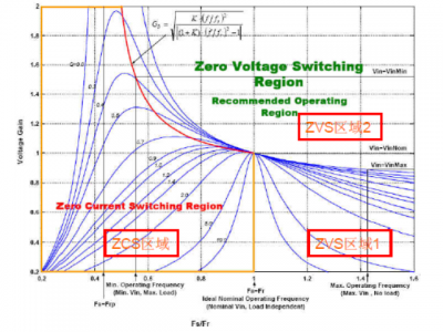
ZVS can be achieved in the entire inductive region, but ZCS of the secondary rectifier cannot be turned off in the ZVS1 region, and there is a reverse recovery problem.
In the ZVS2 region, the ZCS turn-off of the secondary rectifier can be realized, and there is no reverse recovery problem.
Therefore, there are different opinions on choosing to work in the ZVS1 or ZVS2 region.
Theoretically speaking, the efficiency of working in the ZVS2 region is higher than that of the ZVS1 region. The closer it is to the resonance point, the higher the operating point efficiency, while taking into account short-circuit performance and other issues.
3. Is the LLC primary MOSFET ZVS off or ZCS off?
The LLC works in the inductive region, so the turn-on is ZVS, but the turn-off is neither ZVS nor ZCS, it is a hard-switched turn-off, and losses are unavoidable. But for MOSFETs, turn-on losses are much larger than turn-off losses. The ZVS of the LLC refers to the ZVS at the turn-on time, so the switching loss can be greatly reduced.
4. Why use half the bus voltage when calculating LLC turns ratio?
When we calculate a flyback or forward circuit, the bus voltage is used to design the turns ratio, but why does LLC only use half the bus voltage to calculate the turns ratio?
During the half cycle when the LLC upper tube is turned on, the bus bar inputs energy to the LLC network, and a part of this energy is directly transferred to the output. The other part is stored in the network, and relies on the resonant capacitor and resonant inductor to output energy during the half cycle of the lower tube being turned on.
Therefore, only the first half cycle of the bus input energy to the network, that is, the utilization rate of time is half, which is equivalent to 1/2 of the utilization rate of the input voltage.
5. What are the advantages and disadvantages of LLC split resonant capacitors?
In the LLC half-bridge resonant circuit, according to the different connection methods of the resonant capacitors, there are two connection methods in a typical LLC resonant circuit. The difference lies in the connection of the LLC resonant cavity.
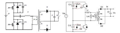
The figure on the left uses a single resonant capacitor Cr, and the input current ripple and current RMS are high, but the wiring is simple and the cost is relatively low.
The figure on the right uses split resonant capacitors C1 and C2, and the input current ripple and current RMS are low. Only half of the rms current flows through C1 and C2, respectively, and the capacitance is only half of the single resonant capacitor in the left figure. In comparison, the split resonance has little advantage.
6. What are the advantages and disadvantages of LLC standalone resonant inductors and integrated resonant inductors?
Integrated resonant inductor, this method uses the primary leakage inductance of the transformer to make the resonant inductor.
The advantages are small size and low cost. The disadvantage is that the leakage inductance is difficult to control, the resonance parameters are not easy to adjust, and the performance is difficult to achieve optimal.
The independent resonant inductor is an external resonant inductor, and the leakage inductance of the main transformer is controlled within a very small range at the same time.
The advantage is that it is easy to adjust the low ratio of the resonance inductance to the excitation inductance, and it is more flexible to optimize and easy to adjust to an ideal state.
The disadvantage is that a resonant inductance is added to increase the volume, and the wiring difficulty and cost increase.
Therefore, power supplies with lower power are generally more willing to use integrated resonant inductors, and the cost is relatively low, while those with large power are more willing to use external resonant inductors, and the performance is easy to optimize.
7. Can the switch tubes of the LLC be directly connected in parallel?
The Miller capacitance Cgd is a parasitic capacitance between the gate and the drain for a MOSFET.
For a hard-switched circuit, the drive current charges Cgs and Cgd and starts to turn on, and during turn-on, the Vds voltage drops, so Cgd starts to discharge.
At this time, a large driving current is required to charge Cgd, which will cause a short plateau in the driving voltage waveform, which is the so-called Miller plateau.
When turned off, the DS voltage rises sharply, and the DG capacitor will flow through the current to charge the GS capacitor, causing secondary conduction.
To eliminate the Maitreya effect at the turn-on time, the DS voltage is zero when the switch is about to turn on, that is, ZVS.
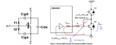
For LLC, the switch tube is turned on by ZVS, so the switch tube with slightly larger power can be directly connected in parallel, there is no Maitreya effect or the Miller effect is minimized.
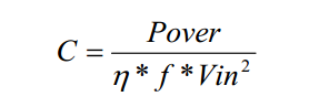
8. What is the relationship between the resonant capacitance of the LLC and the output power?
Let’s use a formula here. Obviously, the larger the power, the larger the resonant capacitor capacity is.
9. What are the two necessary conditions to satisfy ZVS?
The premise of ZVS is that the voltage leads the current, so the LLC must be in the inductive region over the entire load range.
This is the most basic condition, and there is another condition that is often overlooked.
To realize the ZVS of the switch, the peak current im of the excitation inductor must discharge the junction capacitance of the switch that is about to be turned on within the dead time.
Until the power is discharged, the voltage drops to zero, and the switch tube that has been turned off simultaneously charges its junction capacitance to the input voltage.
Therefore, in order to realize ZVS of the two power switches, the relationship between the peak current Ipk of the excitation inductance and the dead time should be satisfied as follows.
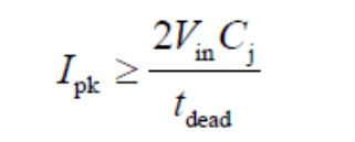
Among them, Vin is the input bus voltage, Cj is the junction capacitance of the MOSFET, and tdead is the dead time.
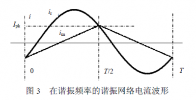
When the circuit works at the resonant frequency, the resonant network current is a sine wave as shown in the figure, where im is the excitation current. At the end of each half switching cycle, the excitation current reaches a maximum value equal to the resonant network current ir.
The peak current of the magnetizing inductance can be obtained as:
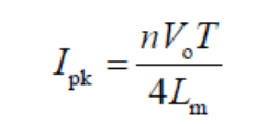
Among Vo is the output voltage, T is the switching period, Lm is the excitation inductance, and the value to Lm should satisfy:
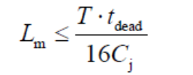
The maximum magnetizing inductance Lm obtained by the inequality can guarantee the ZVS of the switch tube, however, a small Lm will increase the switching loss of the MOSFET.
Due to this passive Lm load, it can be guaranteed to work under zero voltage switching state under any load condition.