Check PCB to Improve SMT Mounting Quality
Jul 15,2024 | Dilong Charger
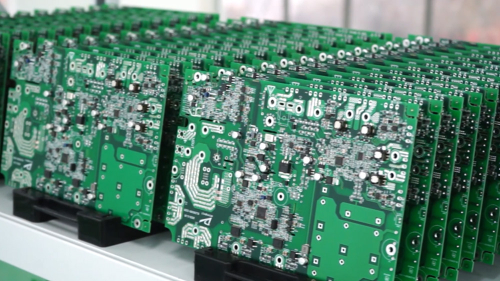
SMT surface mounting technology refers to a technical method of directly installing electronic components on a PCB circuit board, which has the characteristics of full automation, precision, and speed.
To meet the requirements of SMT surface mounting processing, PCB incoming materials need to be inspected according to standards before surface mounting to effectively ensure product quality. So, what are the requirements for PCB incoming materials?

- Appearance requirements for PCB board
The PCB board should not have warping or unevenness, and the appearance should be smooth and flat, otherwise the substrate may have defects such as cracks, scars, rust spots, etc.
When using cleaning agents on PCBs, there should be no adverse reactions. Immerse them in liquid for 5 minutes, and the surface should not produce any adverse reactions and have good impact resistance.
- PCB size and shape requirements
Different SMT equipment has different requirements for PCB size. When designing a PCB, it is necessary to consider the maximum and minimum mounting size of the SMT equipment's PCB, which is generally between 50mm* 50mm-350mm*250mm.
Due to the coefficient of thermal expansion, when the component is less than 3.2mm*1.6mm, it only experiences partial stress. When the component is greater than 3.2mm*1.6mm, attention must be paid to the influence of the coefficient of thermal expansion, and the bending strength of the PCB board must reach 25kg/mm or more to meet SMT mounting standards.
- PCB design requirements
Requirements for Mark Points on PCB Board for SMT
The shape standards for Mark points include circles, squares, and triangles, with sizes ranging from 1.0mm to 2.0mm. The surface is required to be flat, smooth, free of oxides and dirt, and there should be no green oil or other obstacles within 1mm around the Mark point, which should have a significant color difference from the Mark point.
The position of the Mark point should be at least 3mm away from the edge of the board, and there should be no similar Mark points, via holes, test points, etc. within 5mm around it. To avoid incorrect direction of board entry during production, the difference in position between the Mark points on the left and right sides of the PCB and the board edge should be at least 10mm.
SMT surface mounting requires PCB board layout design with a board edge width of 3mm-5mm, spacing of 1.6mm or more, upward bending less than 1.2mm, downward bending less than 0.5mm, and maximum PCB distortion height ÷ diagonal length<0.25. V-shaped grooves, stamp holes, or punching grooves can be used between the plates. It is recommended to use only one method of dividing the same plate. For partially fully surface assembled double-sided surface mounting panels, a combination layout design can be adopted, which allows the use of the same screen, saves programming and line changing time, and improves production efficiency.

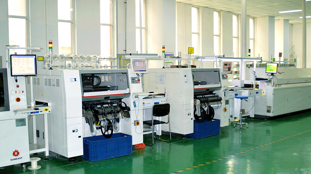
As a well-known supplier of global electric vehicle on-board chargers, on-board DCDC converters and other on-board power products, Dilong New Energy has taken the lead in introducing SMT surface mount technology in the industry and equipped with SMT fully automated SMT production lines, achieving mass production of on-board chargers, on-board DCDC converters and other products earlier. During the product development and production process, Dilong New Energy strictly controls the incoming PCB materials and inspects the PCB boards according to standards before production, effectively ensuring product quality. The product quality is highly welcomed and recognized by the market.


